
PCB designs come with numerous interlinked boards that are connected with computer tools to aid hierarchy, intraboard connectivity, and drawing apps. Many times, this may disrupt collaboration between various system processes hence restricting optimization of system design.
Xpedition multi-board design enhances design functionality while minimizing the cost of development. This is actualized by substituting non-effective manual procedures with fully integrated, automated, and associated workflow. This process eases designers’ work by allowing integration between automated connectors and different levels of abstraction.


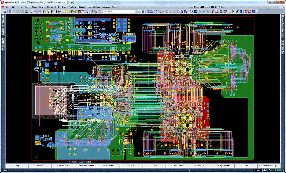
Xpedition multi-board systems design is a fully collateral combined design environment which incorporates different teams, enabling them to work, and help companies achieve spontaneous and scalable technologies to develop combative and inventive products.
When comparing Multi-Board Versus Multilayer Designs, one is likely to realize that they are both important in various applications. In addition, they help design teams in creating various types of PCBs.
Multi-boards come with various benefits which include:
- Ensure that IP is spread across the organization
- Reduce cost of compliance while cutting down enterprise uncertainties in relation to reliability and the security of product
- Encourage discipline and collaboration among the design team
- Aids the regulation of design scale and intricacy
- Eradicates team redundancy, encourages compatibility, and augments team productivity
- Enhances product dependability and functionality
- Minimizes design errors
- Ensures IP application and security
- Eradicates the black box method and incorporates digital domains
Multilayer PCB comes with more than two layers. It differs from the double-sided PCB in that the latter comes with two conductive layers while multilayer PCBs have three conductive layers inserted within the material center.
Development of Multilayer PCBs
Designers laminate wavering layers of core materials and prepreg together and expose them to high pressure and temperature. The main objective of this procedure is to release air between the layers. Resin is then used to epitomise the conductors while the gummy that holds together the layers is melted and alleviated. The materials used vary from Teflon, exotic ceramic, and epoxy glass.
Advantages of Multilayer PCBs
- They have a high assembly density
- Offer increased scalability
- Are small in size which helps save space
- Do not need a wide range of interconnection wiring. This makes them light
- They come with easy to incorporate features
There are some multilayer PCB downsides which include:
- Manufacturing them takes a longer time and is quite expensive
- Cost of maintenance is high and their repairs can be intricate
Multilayer PCBs are useful in various applications such as; file servers, data storage, satellite systems, handheld gadgets, heart monitors, fiber optic receptors, weather analysis, centralized fire alarm systems, X-ray equipment, cell phone repeaters, and computers.
Determining Multilayer PCBs
Individuals can establish the number of layers a PCB has by:
Use a flashlight to check the edges for any signal traces of the copper planes. However, this may not work if the copper is far from the edge. The light can help one establish the possibility of inner layers in the absence of blind vias. Unlike in the first option, execute this on the side where the planes or traces are invisible.
Depending on the manufacturer, one may notice labels for each layer on the board.